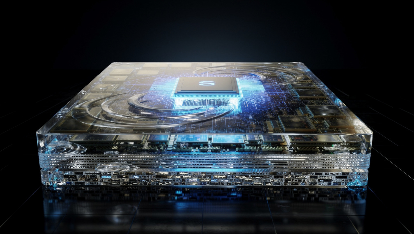
Comparison - Semiconductors

WATS Fabrication
vs The Fab

Seven patents: WATS machine, LPCS wafer, EdgeMemory, EdgeModem, EdgeSemi, EdgeWave, EdgeEDA. Every one eliminates a billion-dollar dependency.

EnergySemiconductorsComputingConsumerHealthDefenseInfrastructureConstructionSecurity
Patent 10 of 66USPTO #64/036,330
EdgeWATS Machine
Wavelength-Addressed Trigger System. Desktop molecular fabrication. 52 sources. Single passive dichroic combiner. Stage moves - turret never rotates. 25,000+ validated recipes.
MetricWATS MachineASML EUV LithographyConventional CVD/ALD
Physical
Size12 x 12 x 12 inches V110m x 5m x 3mRoom-scale multiple chambers
WeightDesktop - under 50 lbs180 tonsHundreds to thousands of lbs
CostLease - no $20B fab required$350M machine + $20B+ fab$1M-$50M per system
InstallationPlug in. Run a recipe.40 containers, 13 months, cleanroomMonths - controlled environment
Capability
Critical DimensionSub-1nm via e-beam slot~2nm minimum~5-10nm typical
Materials2D semis, graphene, diamond, perovskite, MOFs, biological - all in one runSilicon onlyOne material per system
Recipe Library25,000+ validated - target 1,000,000+Fixed process - no recipesFixed per system
LocationAny building - any country - any climateSeismically stable + ultra-pure water + military cleanroomControlled environment required
WATS wins by every measure.Desktop vs 180 tons. Sub-1nm vs 2nm. Any material vs silicon only. Any location vs $20B fab.
Patent 9 of 66USPTO #64/036,328
LPCS Wafer
Latent Pre-loaded Chemistry Stack Wafer. All fabrication chemistry volumetrically pre-loaded. Zero external chemical introduction after manufacture.
MetricLPCS WaferConventional Silicon WaferEUV Photomask
ChemistryFull stack pre-loaded at manufacture - inside the waferBare substrate - all chemistry externalPattern only - no chemistry
External Chemical StepsZero after wafer manufactureDozens of external stepsRequires separate wafer + chemicals
ActivationWavelength-specific photon triggers each layer independentlyTemperature, plasma, reactive gas separatelyUV exposure - no chemistry
Contamination RiskNear zero - sealed chemistry insideHigh - every external step risks contaminationN/A
PortabilityShips as passive wafer - activates only on WATSRequires fab presentRequires lithography system
LPCS Wafer wins.All chemistry pre-loaded. Zero external chemical steps. Ships passive. Activates on WATS only.
Patent 14 of 66USPTO #64/060,215
EdgeMemory
MoS2 ferroelectric FET non-volatile memory. HZO gate dielectric. 2 nanosecond switching. Non-volatile. On-die. 2 petabytes.
MetricEdgeMemory FeFETBest NVMe SSDDRAM DDR53D NAND Flash
Switching Speed2 nanoseconds~200,000 nanoseconds~10ns - volatile~100,000 nanoseconds
Non-VolatileYes - holds data forever without powerYesNo - loses on power lossYes
Speed vs NVMe100,000x fasterBaseline20x faster but volatile2x faster
EnduranceUnlimited - no wear mechanism~3,000 write cyclesUnlimited - no write wear~3,000 cycles
IntegrationOn-die with processor - zero cableSeparate M.2 componentSeparate DIMMSeparate component
EdgeMemory wins.100,000x faster than NVMe. Non-volatile. On-die. No cable. No controller. No bottleneck.
Patent 16 of 66USPTO #64/060,415
EdgeModem EM-1
2D semiconductor monolithic RF transceiver. 5G NR Sub-6 + mmWave. WiFi 7. BT 5.4. GPS. Post-quantum encrypted baseband.
MetricEdgeModem EM-1Qualcomm Snapdragon X80Intel 5G Modem
SubstrateMoS2 - zero silicon - WATS grownSilicon TSMC 4nmSilicon
EncryptionPost-quantum baseband - ML-KEM-1024 hardware enclaveConventional - quantum vulnerableConventional
IntegrationMonolithic single-die - all RF on MoS2Multiple dies - silicon + GaAsMultiple components
5G BandsSub-6 + mmWave full global coverageSub-6 + mmWaveSub-6 only
WiFiWiFi 7 - 46 Gbps theoreticalWiFi 7WiFi 6E
EdgeModem wins.Post-quantum hardware encryption. MoS2 vs silicon. Monolithic vs multi-die. Quantum-proof today.
Patent 50 of 66USPTO #64/067,648
EdgeSemi
Floating freight vehicle. Ion vertical propulsion. WATS superconducting MHD horizontal. Multi-trailer. Zero road contact. Zero emissions.
MetricEdgeSemi FreightDiesel 18-WheelerTesla Semi Electric
Road ContactZero - floats above surfaceFull contact - 80,000 lb road loadFull contact
Road DamageZeroMajor - primary cause of road deteriorationMajor
EmissionsZero - no combustionDiesel exhaust - PM2.5, NOx, CO2Zero operational
RangeEdgeBattery + EdgeSolar - indefinite~1,500 miles per tank~500 miles per charge
Moving PartsZero - ion + MHD propulsionThousandsHundreds
EdgeSemi wins.Zero road contact. Zero road damage. Zero emissions. Zero moving parts. Indefinite range.
Patent 51 of 66USPTO #64/067,649
EdgeWave
Three-layer maritime wave energy degradation. Diaphene deflector vanes, bow cancellation field, ion stabilization.
MetricEdgeWaveShip StabilizersFixed Platform Mooring
Wave AttenuationThree layers - deflector + field cancellation + ion stabilizationSingle - fin stabilizers or ballastStatic mooring - no attenuation
Moving PartsZero - field-based + passive vanesFin actuators - hydraulicNone - passive
Coverage360 degrees - all wave directionsRoll axis primarilyNone
Storm PerformanceActive cancellation scales with wave energyPassive - limited stormMooring strength limit
EdgeWave wins.Three-layer active cancellation. 360 degree. Scales with storm severity. Zero moving parts.
Patent 52 of 66USPTO #64/067,650
EdgeEDA
AI-native EDA platform. Replaces Synopsys and Cadence. Natural language input. WATS fabrication output.
MetricEdgeEDASynopsys Design CompilerCadence Innovus
Input MethodNatural language - speak or type the designManual RTL Verilog codeManual RTL Verilog code
TargetMoS2 2D semiconductor nativeSilicon onlySilicon only
License CostSovereign - no external dependency$500K-$2M+ annual$500K-$2M+ annual
OutputWATS recipe file - direct to fabGDSII - requires external fabGDSII - requires external fab
Silicon DependencyZero100%100%
EdgeEDA wins.Natural language input. MoS2 native. No $2M license. Outputs to WATS fabrication directly.