Semiconductor Fabrication
EDGEWATS
VS EUV LITHOGRAPHY
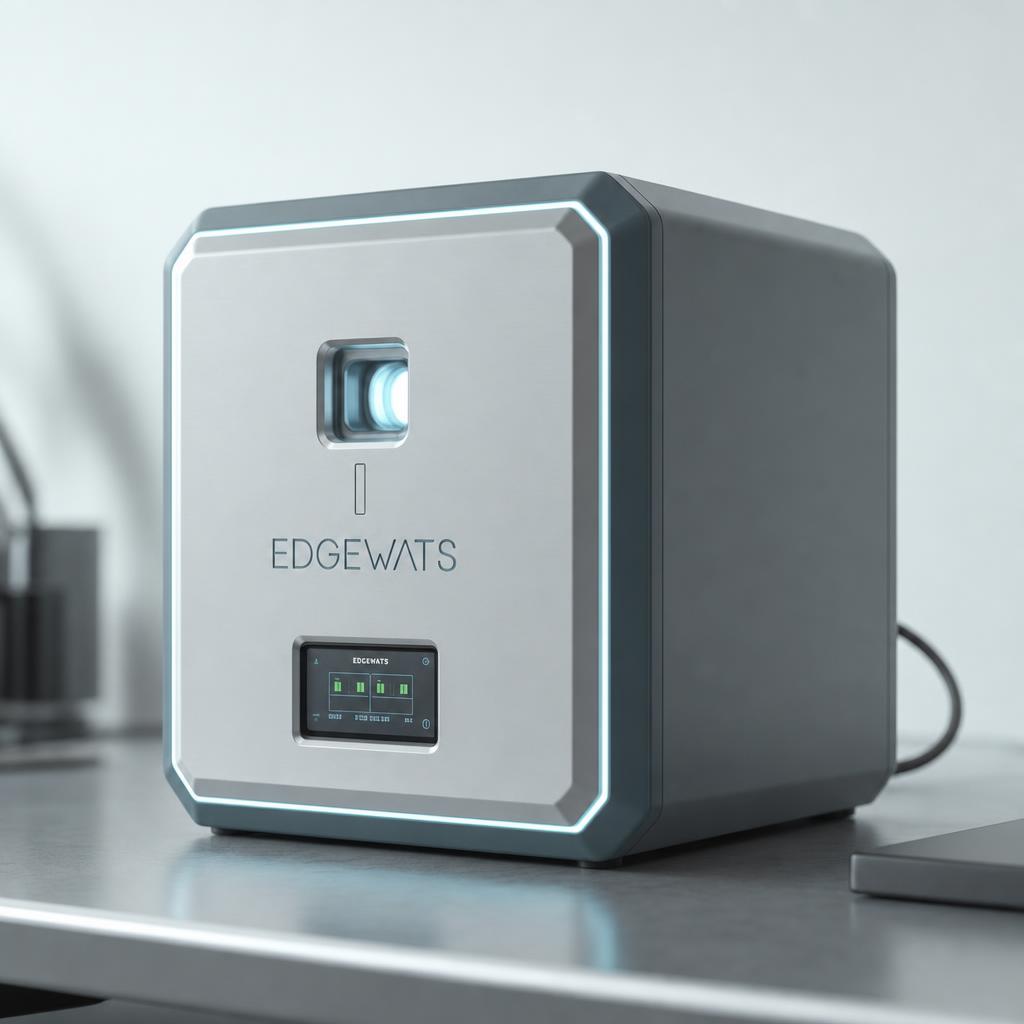
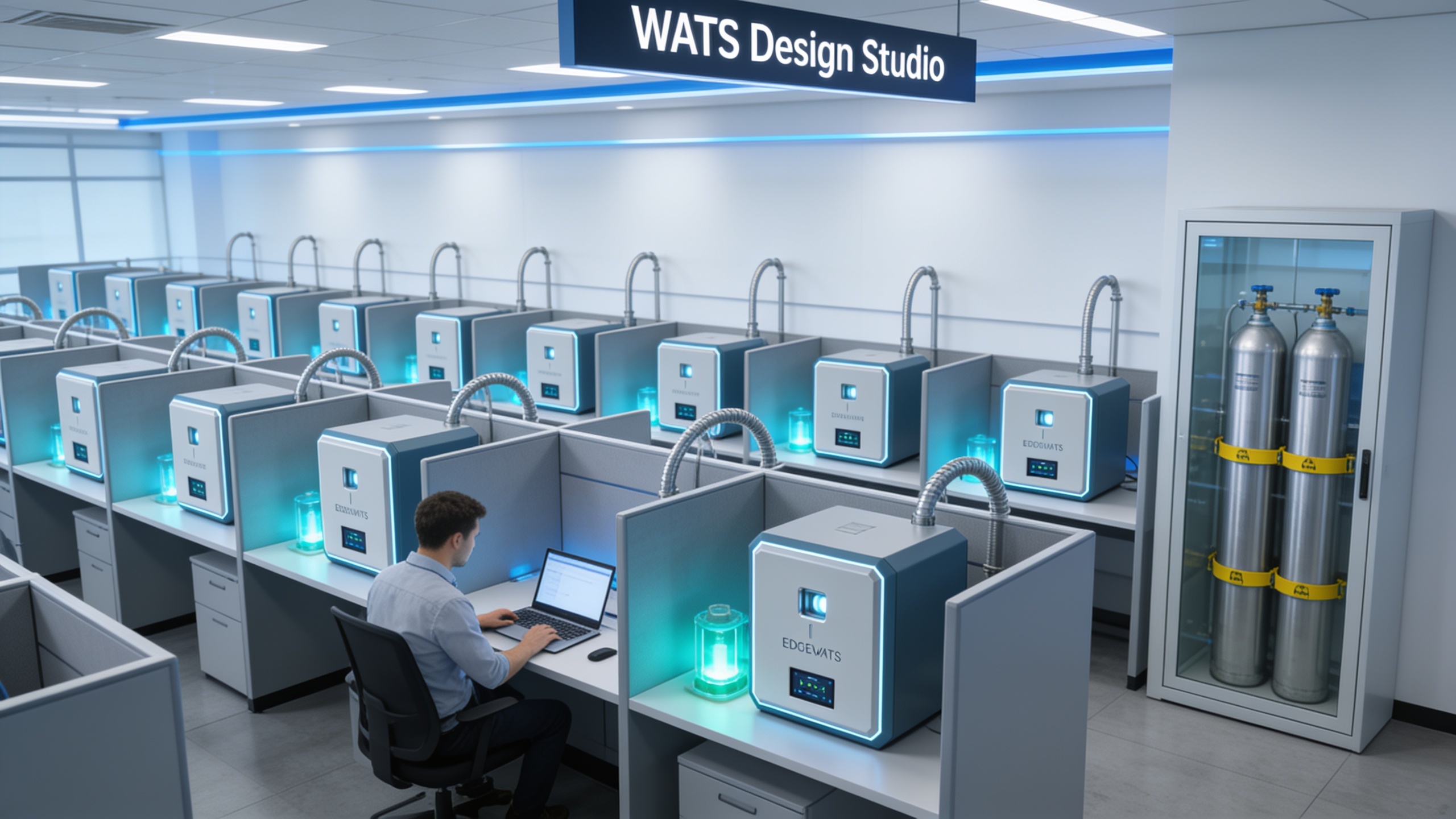
ASML's EUV systems are the most expensive machines ever built — $380M per unit, requiring a dedicated cleanroom, photomasks costing $500K each, and a global supply chain spanning 5,000 components from 800 suppliers. EdgeWATS is a desktop machine. No mask. No cleanroom. One recipe file.
| Metric | EdgeWATS V1 | ASML EUV (NXE:3600D) | ASML DUV (ArF Immersion) | E-Beam Direct Write |
|---|---|---|---|---|
| Unit Cost | Desktop scale — fraction of EUV cost | ~$380M per system | ~$80M per system | $5M–$50M per system |
| Feature Resolution | <1nm — sub-angstrom via HHG + e-beam slots | ~13.5nm EUV wavelength — ~2nm patterned | ~193nm DUV — ~7nm patterned with multi-patterning | Sub-10nm — but very slow throughput |
| Photomask Required | None — wavelength-addressed direct write | Yes — $300K–$500K per mask set | Yes — $50K–$100K per mask set | No — direct write |
| Cleanroom Required | No — WATS operates in controlled atmosphere | Yes — ISO Class 1, massive infrastructure | Yes — ISO Class 1 | Yes — high vacuum required |
| Silicon Substrate | Not required — grows 2D materials on any substrate | Yes — silicon wafer only | Yes — silicon wafer only | Yes — silicon or specialty substrate |
| Materials Supported | MoS₂, graphene, hBN, perovskite, GaO, and 100+ more | Silicon, SiGe, limited III-V | Silicon, SiGe, limited III-V | Silicon and some III-V |
| Recipe Library | 55,000+ peer-reviewed R-recipes — growing to 1M+ | Proprietary process library — not transferable | Proprietary process library — not transferable | Proprietary — tool-specific |
| Multi-Material in One Run | Yes — 52 slots address different materials sequentially or simultaneously | No — one material system per lithography step | No — separate deposition tools required | No — patterning only, deposition separate |
| Supply Chain | Self-contained — EdgeWATS is the supply chain | 800+ suppliers, 5,000+ components, global dependency | Hundreds of suppliers — global | Multiple vendors — less complex than EUV |
| Domestic Availability | Yes — US-designed, US-fabricated | Netherlands only — export controlled | Netherlands only — export controlled | US vendors exist — limited capability |
Thin Film Deposition
EDGEWATS
VS DEPOSITION METHODS
CVD, ALD, MBE, PVD — each is a single-modality tool requiring a separate piece of equipment, a separate facility, and a separate process step. EdgeWATS replaces all of them. Every deposition chemistry is a recipe slot. Every material is a wavelength address.
| Metric | EdgeWATS | CVD / MOCVD | ALD (Atomic Layer Deposition) | MBE (Molecular Beam Epitaxy) |
|---|---|---|---|---|
| Process Temperature | Room temperature — photochemical activation | 600°C–1200°C — high thermal budget | 150°C–400°C | 400°C–800°C — ultra-high vacuum |
| Materials per Machine | 100+ — recipe-defined, any slot combination | 1–3 — tool-specific chemistry | Dozens — but one at a time, slow | 1–2 — ultra-specific to machine config |
| Deposition Rate | Tunable per recipe — simultaneous multi-layer | Fast — high throughput | Very slow — one atomic layer per cycle | Very slow — atom-by-atom |
| Conformality | 3D addressable — beam geometry defines deposition zone | Good for planar, poor for high-aspect-ratio | Excellent — follows any geometry | Line-of-sight only |
| Vacuum Required | Controlled atmosphere — not high vacuum | Low to moderate vacuum | Low to moderate vacuum | Ultra-high vacuum — 10⁻¹¹ Torr |
| Patterning Integrated | Yes — WATS deposits AND patterns in same run | No — requires separate lithography step | No — blanket deposition only | No — separate patterning required |
| 2D Material Growth | Native capability — MoS₂, graphene, hBN, TMDs | Possible but high temp — damages 2D layers | Partial — limited 2D material support | Yes — but ultra-slow and ultra-expensive |
| Machine Footprint | V1: 12×12×12 inches | Room-sized — dedicated facility | Room-sized — dedicated facility | Very large — ultra-high vacuum chamber |
55,000+ Recipes
Every R-recipe in the EdgeWATS library has a traceable peer-reviewed literature source. Parameters are not estimates — they are published, validated process conditions. The library is growing toward 1,000,000. No other fabrication system in the world has a unified cross-material recipe database in a single queryable format.
1M+
target recipe count
Seven Generations. One Physics.
EdgeWATS scales from a desktop enclosure to a facility-scale fabrication platform — same photochemical physics, same recipe format, same beam architecture at every size. ASML's EUV requires a crane and a dedicated building at every node.
V1 — 12×12×12 inches (desktop)
V2 — 24×24×24 inches
V3 — 36×36×36 inches
V4 — 12×12×12 feet
V5 — 12×24×24 feet
V6 — 24×50×50 feet
V7 — 24×100×100 feet
V1 — 12×12×12 inches (desktop)
V2 — 24×24×24 inches
V3 — 36×36×36 inches
V4 — 12×12×12 feet
V5 — 12×24×24 feet
V6 — 24×50×50 feet
V7 — 24×100×100 feet
V1–V7
desktop to facility scale
Self-Improving
EdgeWATS fabricates its own phononic crystal combiner in Phase 2. The machine that builds chips eventually builds a better version of itself. The long-term loop: WATS builds EdgeChip, EdgeChip replaces WATS control computer, WATS builds better EdgeChip. No external fab ever required again.
∞
improvement loop iterations
Fab Infrastructure
EDGEWATS
VS FAB INFRASTRUCTURE REQUIREMENTS
Building a conventional semiconductor fab costs $10B–$20B and takes 3–5 years before a single wafer ships. TSMC's Arizona fab cost $40B. Intel Ohio is $20B. EdgeWATS changes every number in that equation.
| Metric | EdgeWATS System | TSMC 3nm Fab (Arizona) | Intel Ohio Fab | Samsung Texas Fab |
|---|---|---|---|---|
| Capital Cost | Desktop machine — not a building | $40B+ total investment | $20B+ planned | $17B+ |
| Build Time to First Wafer | EdgeWATS ships — recipe loads — run starts | 3–5 years construction + qualification | 3+ years (delayed multiple times) | 3+ years |
| Cleanroom Required | No | Yes — millions of sq ft ISO Class 1 | Yes — massive facility | Yes — massive facility |
| Water Consumption | Minimal — no wet chemical baths | Millions of gallons per day — water crisis risk | Millions of gallons per day | Millions of gallons per day |
| Chemical Waste | Near zero — photochemical process, no wet etch | Massive — hundreds of process chemicals, EPA regulated | Massive chemical waste stream | Massive chemical waste stream |
| Foreign Dependency | None — US-designed, US-built, US-operated | ASML EUV (Netherlands) — single-source dependency | ASML EUV (Netherlands) | ASML EUV (Netherlands) |
| Silicon Required | Never — 2D semiconductor materials only | Yes — prime silicon wafer supply chain | Yes — prime silicon wafer supply chain | Yes — prime silicon wafer supply chain |
| Export Control Risk | None — Edge owns the technology domestically | ASML export license required — US policy dependent | ASML export license dependency | Full US export control exposure |